Huawei chip claim tests US sanctions, Apple and Nvidia
Huawei chip claims point to a design workaround, not clear node parity, as Apple and Nvidia face a harder China market.
Huawei says a new chip-design approach could deliver denser semiconductors within five years. The claim turns a familiar sanctions question into a harder one: is Washington still slowing China’s flagship technology company, or mostly forcing it onto a different route?
The company lays out its answer in the Tau Scaling Law announcement. Density gains, it argues, do not have to come only from shrinking transistors. LogicFolding can shorten signal paths, lift system performance and eventually reach density equivalent to a 1.4 nanometre process by 2031, Huawei says. Matching TSMC, Apple’s foundry partner, or Nvidia’s most advanced manufacturing chain is a much higher bar.
Engineers are not the only audience. Washington, Beijing, Apple, Nvidia and device buyers all want to know whether export controls still set the ceiling on Chinese hardware.
We found a new path.
He Tingbo, Huawei, quoted by Wired
Analysts pushed back quickly. Reuters and CNBC both treated Huawei’s material less as a clean process-node leap than as an attempt to squeeze more work out of constrained tools. That is the useful frame. If the proposal works, its significance comes from the workaround, not from proof that sanctions have failed.
The claim is about density, not full parity
Huawei’s case starts with a technical distinction that is easy to miss. Conventional chip progress has been sold as geometry: make transistors smaller, pack more of them into the same area, then push performance and efficiency forward. Here, the bottleneck is time and layout. Folded logic and shorter interconnects are meant to make a chip behave more like a smaller-node part.

Those gains are not trivial. Huawei said it has designed and mass-produced 381 chips and mapped a density path from 126 million transistors per square millimetre to 155 million, then 238 million. Management presents the upper step as 1.4nm-equivalent density. In a market trained to read node names as status symbols, that phrase will travel.
Asterisk required. Omdia analyst He Hui told Reuters the approach is a shift from node-driven scaling to system-level efficiency scaling, rather than a direct claim of foundry leadership.
What Huawei is proposing is a shift from traditional node-driven scaling to system-level efficiency scaling.
He Hui, Omdia, quoted by Reuters
For Australian CIOs and device buyers, the distinction is practical. Node labels do not run workloads by themselves. Yield, heat, power draw, design-tool maturity and packaging reliability decide whether a clever architecture becomes a dependable phone chip or AI accelerator. The Register was blunt on this point, treating the claim as packaging-led marketing until independent silicon proves otherwise.
The first proof point is Kirin, not the keynote
Product evidence comes next. CNBC reported that Huawei plans to use LogicFolding in Kirin smartphone chips this fall, with Ascend AI parts and cluster products following later. That sequence gives the market something more concrete than a conference slide.
Smartphone silicon can absorb some compromises through software tuning, modem integration and battery management. A data-centre AI accelerator is less forgiving. If Tau Scaling is to be read as a strategic break from the 7nm ceiling, Ascend parts need to show repeatable performance at scale, not just a density claim on paper.
In CNBC’s reporting, Paul Triolo, a partner at DGA-Albright Stonebridge Group, put the sceptic’s case plainly.
A stacked/folded design can produce effective density gains, but it does not mean Huawei has solved the full process, yield, power, thermal, and device-performance problems.
Paul Triolo, quoted by CNBC
That is the line between a breakthrough and a bargaining chip. Huawei has reason to show confidence. It also has reason to make the sanctions regime look less decisive than Washington intended. Until third-party benchmarks, teardown evidence and shipping volumes line up, the claim sits in the middle: plausible enough to matter, not proven enough to rewrite the hierarchy.
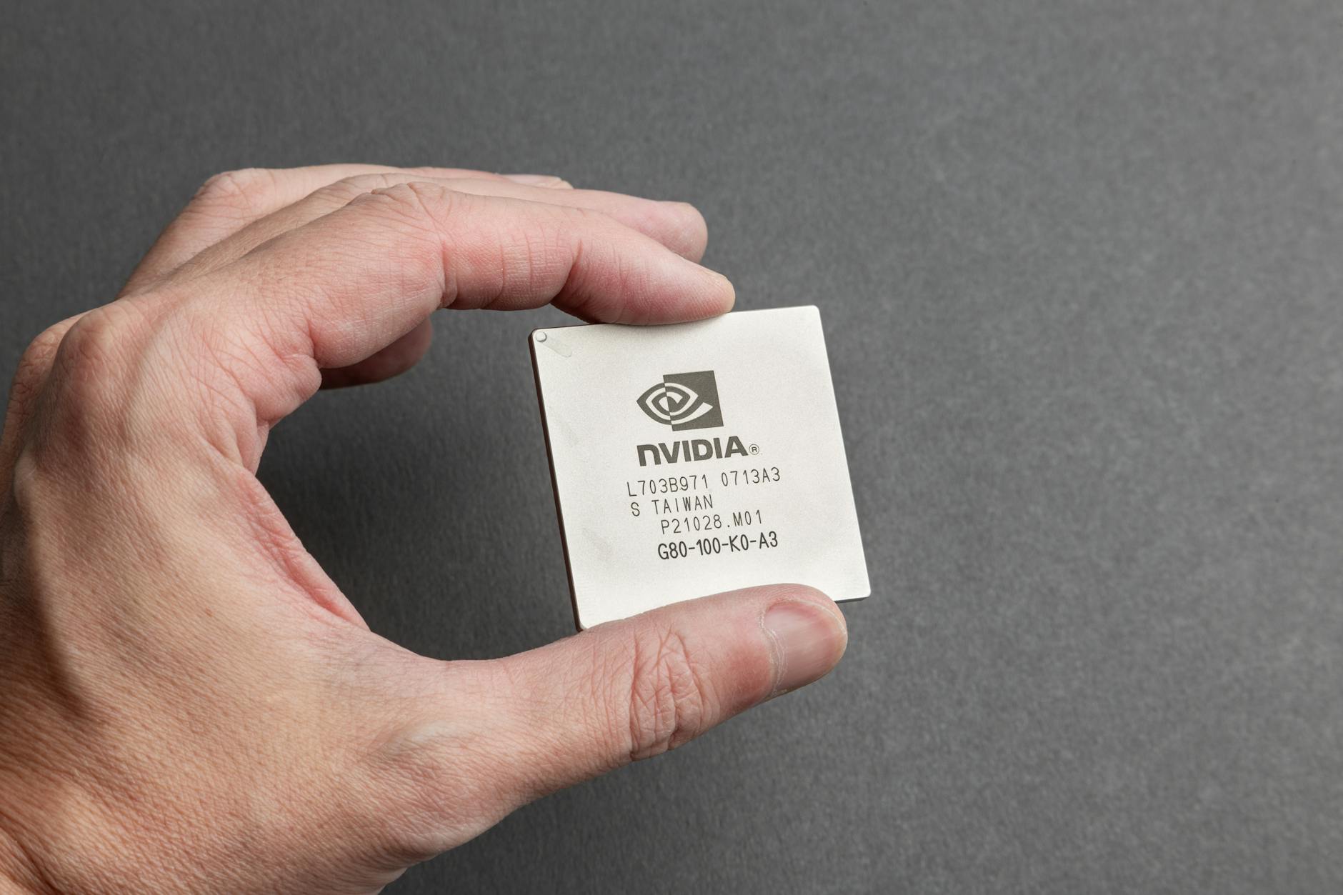
Apple and Nvidia are the commercial audience
Apple feels the Huawei story first in handsets. Reuters reported in March that Apple’s China smartphone sales jumped 23 per cent in the first nine weeks of 2026, bucking the wider market trend. That bounce does not remove the structural pressure. Huawei’s Mate line has shown how quickly Chinese consumer demand can swing toward a domestic champion when hardware, software and national preference align.

A credible Chinese silicon roadmap gives Huawei more control over its premium devices, fewer imported choke points and a stronger pitch to consumers who want a high-end phone built around a domestic stack. It does not have to match the iPhone’s custom silicon overnight to make Apple’s China market harder.
Nvidia faces a sharper version of the same substitution problem. CNBC framed Huawei’s chip-design claim as part of a rivalry that extends into AI accelerators, and Jensen Huang has warned that export rules are pushing China toward local alternatives. Ars Technica later noted Huang’s comment that Nvidia had largely conceded China to Huawei. The wording suggests the China opportunity is no longer just limited by licence approvals; it is being reallocated to suppliers that Beijing can back more easily.
None of this means Huawei can replace Nvidia in global AI training clusters. Software, networking, memory bandwidth and developer adoption still matter. Nvidia’s moat is CUDA and the broader data-centre platform as much as the GPU package. For Chinese government procurement, state-linked cloud projects and companies that cannot rely on US supply, good-enough domestic acceleration can still be enough.
Sanctions are slowing Huawei and training it
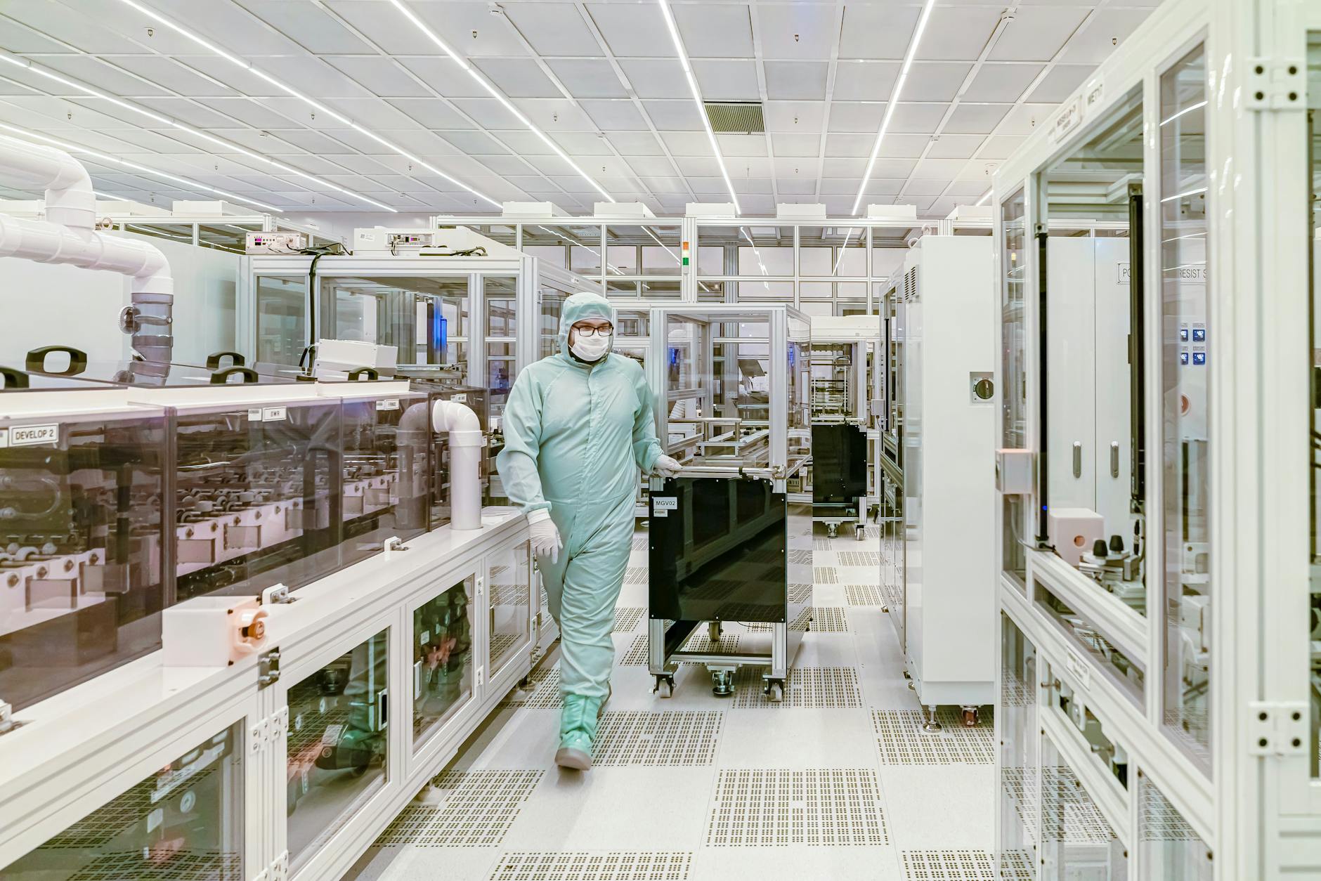
Export controls have clearly constrained Huawei. The company is still trying to work around lithography limits, not demonstrating open access to the same toolchain used by TSMC and Samsung. Reuters has reported that China remains constrained by advanced lithography, and TSMC is targeting 1.4nm mass production in 2028, ahead of Huawei’s 2031 equivalence claim.
Yet restrictions have also forced Huawei to build a more self-contained semiconductor stack. That is the part of the story Washington cannot ignore. A control that slows access to frontier tools can still accelerate domestic design methods, packaging investment and procurement preference. Huawei’s announcement is a public argument that those substitutions are becoming productive.
Wired’s profile of He Tingbo captured that strategic posture: not a victory lap, but a declaration that Huawei will keep changing the problem until its constraints become design inputs. Semafor made a similar point, framing the plan as a bid to rival US capabilities despite current high-end Chinese chips lagging the world’s most advanced parts.
For device buyers outside China, including in Australia, the immediate effect is modest. No one should buy a phone in 2026 on the promise of a 2031 chip roadmap. Enterprises buying AI infrastructure face the broader question. The semiconductor supply chain is splitting into overlapping but politically distinct stacks. Nvidia, Apple and TSMC still define the leading edge, but Huawei is showing how a blocked company can turn the block itself into a product strategy.
The Tau Scaling claim is more than a handset story. It signals that the chip race is no longer only about who prints the smallest node. It is also about who can keep improving when the usual path is closed.
Soren Chau
Enterprise editor covering AWS, Azure, and GCP in the AU region, plus the SaaS shaping local IT. Reports from Sydney.